APO RESEARCH · REPORT
4 Inches GaN Single Crystal Substrate
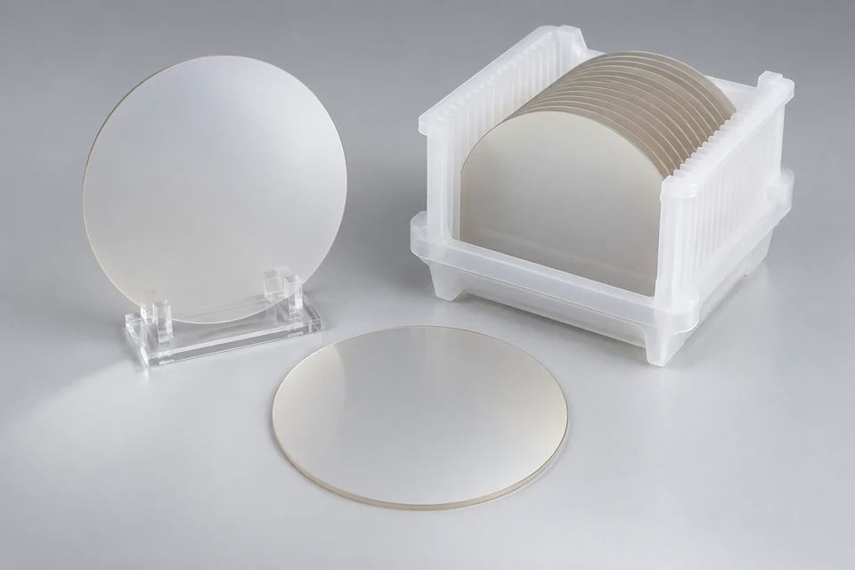
A nominal four-inch single-crystal gallium-nitride substrate supplied for downstream semiconductor processing.
Product & engineering
Understand the product.
Crystal material, orientation, diameter, thickness, defects and surface preparation define the substrate. Bulk GaN, a GaN film on another substrate and a finished device are different supplied objects.
What turns activity into demand
The selected edition segments 4 Inches GaN Single Crystal Substrate by 4 Inch GaN wafers (non-doped); 4 Inch GaN wafers (iron doped). Its application or channel categories include Laser Diodes; Power Electronic Devices; High Frequency Electronic Devices; Others.
The commercial boundary
Read those groups within the selected report’s geography, years and measure. Component, material and finished-system activity should not be combined unless that edition explicitly defines the same commercial scope.
Is this bulk GaN or an epitaxial structure?
Crystal material, orientation, diameter, thickness, defects and surface preparation define the substrate. Bulk GaN, a GaN film on another substrate and a finished device are different supplied objects. The selected edition’s categories describe its research segmentation; a supplier specification and application-level acceptance test define the particular purchased product.
Selected research
Market Structure
Global 4 Inches GaN Single Crystal Substrate Market by Size, by Type, by Application, by Region, History and Forecast 2021-2032
Market perspective
The global 4 Inches GaN Single Crystal Substrate market is projected to grow from US$ million in 2026 to US$ million by 2032, implying a CAGR of % over 2026-2032.
The US & Canada market for 4 Inches GaN Single Crystal Substrate is projected to increase from US$ million in 2026 to US$ million by 2032, at a CAGR of % over 2026-2032.
The Europe market for 4 Inches GaN Single Crystal Substrate is projected to increase from US$ million in 2026 to US$ million by 2032, at a CAGR of % over 2026-2032.
Read the full market overview
The Asia Pacific market for 4 Inches GaN Single Crystal Substrate is projected to increase from US$ million in 2026 to US$ million by 2032, at a CAGR of % over 2026-2032.
The China market for 4 Inches GaN Single Crystal Substrate is projected to increase from US$ million in 2026 to US$ million by 2032, at a CAGR of % over 2026-2032.
Leading global manufacturers of 4 Inches GaN Single Crystal Substrate include Toyoda Gosei, Kyma Technologies, Sumitomo Electric Device Innovations (SEDI) (SCIOCS), Mitsubishi Chemical, Eta Research Ltd, Suzhou Nanowin Science and Technology, Sanan Optoelectronics, Sino Nitride Semiconductor and Goetsu Semiconductor Wuxi, among others. In 2025, the top three vendors together accounted for approximately % of global revenue.
On the production side, the report examines 4 Inches GaN Single Crystal Substrate output, growth rates, and market shares by manufacturer and by region (at regional and country level) for 2021-2026, with forecasts through 2032.
On the consumption side, the report analyzes sales of 4 Inches GaN Single Crystal Substrate by region (regional and country level), company, type, and application for 2021-2026 and provides forecasts through 2032.
The report provides an overview of the global 4 Inches GaN Single Crystal Substrate market in terms of capacity, output, revenue, and price, analyzing global market trends using historical revenue and sales data for 2021-2025, estimates for 2026, and projected CAGRs through 2032.
The study covers key producers of 4 Inches GaN Single Crystal Substrate and consumption patterns in major regions and countries, assesses future market potential, and highlights priority regions and countries for segmenting the market into sub-sectors, with country-specific market value data for the U.S., Canada, Mexico, Brazil, China, Japan, South Korea, Southeast Asia, India, Germany, the U.K., Italy, the Middle East, Africa, and other countries.
The report also presents 4 Inches GaN Single Crystal Substrate sales, revenue, market share, and industry ranking for the main manufacturers for 2021-2026, identifies the major stakeholders in the global market, and analyzes their competitive landscape and market positioning based on recent developments and segmental revenues.
In addition, the report analyzes segment data by type and application—covering sales, revenue, and price—for 2021-2032, and evaluates and forecasts the 4 Inches GaN Single Crystal Substrate market size, projected growth trends, production technologies, key applications, and end-use industries.
4 Inches GaN Single Crystal Substrate Segment by Company
Toyoda Gosei
Kyma Technologies
Sumitomo Electric Device Innovations (SEDI) (SCIOCS)
Mitsubishi Chemical
Eta Research Ltd
Suzhou Nanowin Science and Technology
Sanan Optoelectronics
Sino Nitride Semiconductor
Goetsu Semiconductor Wuxi
BTOZ
4 Inches GaN Single Crystal Substrate Segment by Type
4 Inch GaN wafers (non-doped)
4 Inch GaN wafers (iron doped)
4 Inches GaN Single Crystal Substrate Segment by Application
Laser Diodes
Power Electronic Devices
High Frequency Electronic Devices
Others
4 Inches GaN Single Crystal Substrate Segment by Region
North America
United States
Canada
Mexico
Europe
Germany
France
U.K.
Italy
Russia
Spain
Netherlands
Switzerland
Sweden
Poland
Asia-Pacific
China
Japan
South Korea
India
Australia
Taiwan
Southeast Asia
South America
Brazil
Argentina
Chile
Middle East & Africa
Egypt
South Africa
Israel
Türkiye
GCC Countries
Study Objectives
1. To analyze and research the global status and future forecast, involving, production, value, consumption, growth rate (CAGR), market share, historical and forecast.
2. To present the key manufacturers, capacity, production, revenue, market share, and Recent Developments.
3. To split the breakdown data by regions, type, manufacturers, and Application.
4. To analyze the global and key regions market potential and advantage, opportunity and challenge, restraints, and risks.
5. To identify significant trends, drivers, influence factors in global and regions.
6. To analyze competitive developments such as expansions, agreements, new product launches, and acquisitions in the market.
Reasons to Buy This Report
1. This report will help the readers to understand the competition within the industries and strategies for the competitive environment to enhance the potential profit. The report also focuses on the competitive landscape of the global 4 Inches GaN Single Crystal Substrate market, and introduces in detail the market share, industry ranking, competitor ecosystem, market performance, new product development, operation situation, expansion, and acquisition. etc. of the main players, which helps the readers to identify the main competitors and deeply understand the competition pattern of the market.
2. This report will help stakeholders to understand the global industry status and trends of 4 Inches GaN Single Crystal Substrate and provides them with information on key market drivers, restraints, challenges, and opportunities.
3. This report will help stakeholders to understand competitors better and gain more insights to strengthen their position in their businesses. The competitive landscape section includes the market share and rank (in volume and value), competitor ecosystem, new product development, expansion, and acquisition.
4. This report stays updated with novel technology integration, features, and the latest developments in the market.
5. This report helps stakeholders to gain insights into which regions to target globally.
6. This report helps stakeholders to gain insights into the end-user perception concerning the adoption of 4 Inches GaN Single Crystal Substrate.
7. This report helps stakeholders to identify some of the key players in the market and understand their valuable contribution.
Chapter Outline
Chapter 1: Provides an overview of the 4 Inches GaN Single Crystal Substrate market, including product definition, global market growth prospects, production value, capacity, and average price forecasts (2021-2032).
Chapter 2: Analysis key trends, drivers, challenges, and opportunities within the global 4 Inches GaN Single Crystal Substrate industry.
Chapter 3: Detailed analysis of 4 Inches GaN Single Crystal Substrate market competition landscape. Including 4 Inches GaN Single Crystal Substrate manufacturers' output value, output and average price from 2021 to 2026, as well as competition analysis indicators such as origin, product type, application, merger and acquisition information, etc.
Chapter 4: Provides the analysis of various market segments by type, covering the market size and development potential of each market segment, to help readers find the blue ocean market in different market segments.
Chapter 5: Provides the analysis of various market segments by application, covering the market size and development potential of each market segment, to help readers find the blue ocean market in different downstream markets.
Chapter 6: Provides profiles of key players, introducing the basic situation of the main companies in the market in detail, including product production/output, value, price, gross margin, product introduction, recent development, etc.
Chapter 7: Production/Production Value of 4 Inches GaN Single Crystal Substrate by region. It provides a quantitative analysis of the market size and development potential of each region in the next six years.
Chapter 8: Consumption of 4 Inches GaN Single Crystal Substrate in regional level and country level. It provides a quantitative analysis of the market size and development potential of each region and its main countries and introduces the market development, future development prospects, market space, and production of each country in the world.
Chapter 9: Analysis of industrial chain, including the upstream and downstream of the industry.
Chapter 10: Concluding Insights of the report.
More report detail
Tables and figures
Scope & coverage.
Types
- 4 Inch GaN wafers (non-doped)
- 4 Inch GaN wafers (iron doped)
Applications
- Laser Diodes
- Power Electronic Devices
- High Frequency Electronic Devices
- Others
Companies covered
- Toyoda Gosei
- Kyma Technologies
- Sumitomo Electric Device Innovations (SEDI) (SCIOCS)
- Mitsubishi Chemical
- Eta Research Ltd
- Suzhou Nanowin Science and Technology
- Sanan Optoelectronics
- Sino Nitride Semiconductor
- Goetsu Semiconductor Wuxi
- BTOZ
Inside the report.
1 Market Overview
- 1.1 Product Definition
- 1.2 Global Market Growth Prospects
- 1.2.1 Global 4 Inches GaN Single Crystal Substrate Production Value Estimates and Forecasts (2021-2032)
- 1.2.2 Global 4 Inches GaN Single Crystal Substrate Production Capacity Estimates and Forecasts (2021-2032)
- 1.2.3 Global 4 Inches GaN Single Crystal Substrate Production Estimates and Forecasts (2021-2032)
- 1.2.4 Global 4 Inches GaN Single Crystal Substrate Market Average Price (2021-2032)
- 1.3 Assumptions and Limitations
- 1.4 Study Goals and Objectives
2 Global 4 Inches GaN Single Crystal Substrate Market Dynamics
- 2.1 4 Inches GaN Single Crystal Substrate Industry Trends
- 2.2 4 Inches GaN Single Crystal Substrate Industry Drivers
- 2.3 4 Inches GaN Single Crystal Substrate Industry Opportunities and Challenges
- 2.4 4 Inches GaN Single Crystal Substrate Industry Restraints
3 4 Inches GaN Single Crystal Substrate Market by Manufacturers
- 3.1 Global 4 Inches GaN Single Crystal Substrate Production Value by Manufacturers (2021-2026)
- 3.2 Global 4 Inches GaN Single Crystal Substrate Production by Manufacturers (2021-2026)
- 3.3 Global 4 Inches GaN Single Crystal Substrate Average Price by Manufacturers (2021-2026)
- 3.4 Global 4 Inches GaN Single Crystal Substrate Industry Manufacturers Ranking, 2024 VS 2025 VS 2026
- 3.5 Global 4 Inches GaN Single Crystal Substrate Key Manufacturers Manufacturing Sites & Headquarters
- 3.6 Global 4 Inches GaN Single Crystal Substrate Manufacturers, Product Type & Application
- 3.7 Global 4 Inches GaN Single Crystal Substrate Manufacturers Established Date
- 3.8 Market Competitive Analysis
- 3.8.1 Global 4 Inches GaN Single Crystal Substrate Market CR5 and HHI
- 3.8.2 Global Top 5 and 10 4 Inches GaN Single Crystal Substrate Players Market Share by Production Value in 2025
- 3.8.3 2025 4 Inches GaN Single Crystal Substrate Tier 1, Tier 2, and Tier 3
4 4 Inches GaN Single Crystal Substrate Market by Type
- 4.1 4 Inches GaN Single Crystal Substrate Type Introduction
- 4.1.1 4 Inch GaN wafers (non-doped)
- 4.1.2 4 Inch GaN wafers (iron doped)
- 4.2 Global 4 Inches GaN Single Crystal Substrate Production by Type
- 4.2.1 Global 4 Inches GaN Single Crystal Substrate Production by Type (2021 VS 2025 VS 2032)
- 4.2.2 Global 4 Inches GaN Single Crystal Substrate Production by Type (2021-2032)
- 4.2.3 Global 4 Inches GaN Single Crystal Substrate Production Market Share by Type (2021-2032)
- 4.3 Global 4 Inches GaN Single Crystal Substrate Production Value by Type
- 4.3.1 Global 4 Inches GaN Single Crystal Substrate Production Value by Type (2021 VS 2025 VS 2032)
- 4.3.2 Global 4 Inches GaN Single Crystal Substrate Production Value by Type (2021-2032)
- 4.3.3 Global 4 Inches GaN Single Crystal Substrate Production Value Market Share by Type (2021-2032)
5 4 Inches GaN Single Crystal Substrate Market by Application
- 5.1 4 Inches GaN Single Crystal Substrate Application Introduction
- 5.1.1 Laser Diodes
- 5.1.2 Power Electronic Devices
- 5.1.3 High Frequency Electronic Devices
- 5.1.4 Others
- 5.2 Global 4 Inches GaN Single Crystal Substrate Production by Application
- 5.2.1 Global 4 Inches GaN Single Crystal Substrate Production by Application (2021 VS 2025 VS 2032)
- 5.2.2 Global 4 Inches GaN Single Crystal Substrate Production by Application (2021-2032)
- 5.2.3 Global 4 Inches GaN Single Crystal Substrate Production Market Share by Application (2021-2032)
- 5.3 Global 4 Inches GaN Single Crystal Substrate Production Value by Application
- 5.3.1 Global 4 Inches GaN Single Crystal Substrate Production Value by Application (2021 VS 2025 VS 2032)
- 5.3.2 Global 4 Inches GaN Single Crystal Substrate Production Value by Application (2021-2032)
- 5.3.3 Global 4 Inches GaN Single Crystal Substrate Production Value Market Share by Application (2021-2032)
6 Company Profiles
- 6.1 Toyoda Gosei
- 6.1.1 Toyoda Gosei Company Information
- 6.1.2 Toyoda Gosei Business Overview
- 6.1.3 Toyoda Gosei 4 Inches GaN Single Crystal Substrate Production, Value and Gross Margin (2021-2026)
- 6.1.4 Toyoda Gosei 4 Inches GaN Single Crystal Substrate Product Portfolio
- 6.1.5 Toyoda Gosei Recent Developments
- 6.2 Kyma Technologies
- 6.2.1 Kyma Technologies Company Information
- 6.2.2 Kyma Technologies Business Overview
- 6.2.3 Kyma Technologies 4 Inches GaN Single Crystal Substrate Production, Value and Gross Margin (2021-2026)
- 6.2.4 Kyma Technologies 4 Inches GaN Single Crystal Substrate Product Portfolio
- 6.2.5 Kyma Technologies Recent Developments
- 6.3 Sumitomo Electric Device Innovations (SEDI) (SCIOCS)
- 6.3.1 Sumitomo Electric Device Innovations (SEDI) (SCIOCS) Company Information
- 6.3.2 Sumitomo Electric Device Innovations (SEDI) (SCIOCS) Business Overview
- 6.3.3 Sumitomo Electric Device Innovations (SEDI) (SCIOCS) 4 Inches GaN Single Crystal Substrate Production, Value and Gross Margin (2021-2026)
- 6.3.4 Sumitomo Electric Device Innovations (SEDI) (SCIOCS) 4 Inches GaN Single Crystal Substrate Product Portfolio
- 6.3.5 Sumitomo Electric Device Innovations (SEDI) (SCIOCS) Recent Developments
- 6.4 Mitsubishi Chemical
- 6.4.1 Mitsubishi Chemical Company Information
- 6.4.2 Mitsubishi Chemical Business Overview
- 6.4.3 Mitsubishi Chemical 4 Inches GaN Single Crystal Substrate Production, Value and Gross Margin (2021-2026)
- 6.4.4 Mitsubishi Chemical 4 Inches GaN Single Crystal Substrate Product Portfolio
- 6.4.5 Mitsubishi Chemical Recent Developments
- 6.5 Eta Research Ltd
- 6.5.1 Eta Research Ltd Company Information
- 6.5.2 Eta Research Ltd Business Overview
- 6.5.3 Eta Research Ltd 4 Inches GaN Single Crystal Substrate Production, Value and Gross Margin (2021-2026)
- 6.5.4 Eta Research Ltd 4 Inches GaN Single Crystal Substrate Product Portfolio
- 6.5.5 Eta Research Ltd Recent Developments
- 6.6 Suzhou Nanowin Science and Technology
- 6.6.1 Suzhou Nanowin Science and Technology Company Information
- 6.6.2 Suzhou Nanowin Science and Technology Business Overview
- 6.6.3 Suzhou Nanowin Science and Technology 4 Inches GaN Single Crystal Substrate Production, Value and Gross Margin (2021-2026)
- 6.6.4 Suzhou Nanowin Science and Technology 4 Inches GaN Single Crystal Substrate Product Portfolio
- 6.6.5 Suzhou Nanowin Science and Technology Recent Developments
- 6.7 Sanan Optoelectronics
- 6.7.1 Sanan Optoelectronics Company Information
- 6.7.2 Sanan Optoelectronics Business Overview
- 6.7.3 Sanan Optoelectronics 4 Inches GaN Single Crystal Substrate Production, Value and Gross Margin (2021-2026)
- 6.7.4 Sanan Optoelectronics 4 Inches GaN Single Crystal Substrate Product Portfolio
- 6.7.5 Sanan Optoelectronics Recent Developments
- 6.8 Sino Nitride Semiconductor
- 6.8.1 Sino Nitride Semiconductor Company Information
- 6.8.2 Sino Nitride Semiconductor Business Overview
- 6.8.3 Sino Nitride Semiconductor 4 Inches GaN Single Crystal Substrate Production, Value and Gross Margin (2021-2026)
- 6.8.4 Sino Nitride Semiconductor 4 Inches GaN Single Crystal Substrate Product Portfolio
- 6.8.5 Sino Nitride Semiconductor Recent Developments
- 6.9 Goetsu Semiconductor Wuxi
- 6.9.1 Goetsu Semiconductor Wuxi Company Information
- 6.9.2 Goetsu Semiconductor Wuxi Business Overview
- 6.9.3 Goetsu Semiconductor Wuxi 4 Inches GaN Single Crystal Substrate Production, Value and Gross Margin (2021-2026)
- 6.9.4 Goetsu Semiconductor Wuxi 4 Inches GaN Single Crystal Substrate Product Portfolio
- 6.9.5 Goetsu Semiconductor Wuxi Recent Developments
- 6.10 BTOZ
- 6.10.1 BTOZ Company Information
- 6.10.2 BTOZ Business Overview
- 6.10.3 BTOZ 4 Inches GaN Single Crystal Substrate Production, Value and Gross Margin (2021-2026)
- 6.10.4 BTOZ 4 Inches GaN Single Crystal Substrate Product Portfolio
- 6.10.5 BTOZ Recent Developments
7 Global 4 Inches GaN Single Crystal Substrate Production by Region
- 7.1 Global 4 Inches GaN Single Crystal Substrate Production by Region: 2021 VS 2025 VS 2032
- 7.2 Global 4 Inches GaN Single Crystal Substrate Production by Region (2021-2032)
- 7.2.1 Global 4 Inches GaN Single Crystal Substrate Production by Region (2021-2026)
- 7.2.2 Global 4 Inches GaN Single Crystal Substrate Production Forecast by Region (2027-2032)
- 7.3 Global 4 Inches GaN Single Crystal Substrate Production by Region: 2021 VS 2025 VS 2032
- 7.4 Global 4 Inches GaN Single Crystal Substrate Production Value by Region (2021-2032)
- 7.4.1 Global 4 Inches GaN Single Crystal Substrate Production Value by Region (2021-2026)
- 7.4.2 Global 4 Inches GaN Single Crystal Substrate Production Value by Region (2027-2032)
- 7.5 Global 4 Inches GaN Single Crystal Substrate Market Price Analysis by Region (2021-2032)
- 7.6 Regional Production Value Trends (2021-2032)
- 7.6.1 North America 4 Inches GaN Single Crystal Substrate Production Value (2021-2032)
- 7.6.2 Europe 4 Inches GaN Single Crystal Substrate Production Value (2021-2032)
- 7.6.3 Asia-Pacific 4 Inches GaN Single Crystal Substrate Production Value (2021-2032)
- 7.6.4 South America 4 Inches GaN Single Crystal Substrate Production Value (2021-2032)
- 7.6.5 Middle East & Africa 4 Inches GaN Single Crystal Substrate Production Value (2021-2032)
8 Global 4 Inches GaN Single Crystal Substrate Consumption by Region
- 8.1 Global 4 Inches GaN Single Crystal Substrate Consumption by Region: 2021 VS 2025 VS 2032
- 8.2 Global 4 Inches GaN Single Crystal Substrate Consumption by Region (2021-2032)
- 8.2.1 Global 4 Inches GaN Single Crystal Substrate Consumption by Region (2021-2026)
- 8.2.2 Global 4 Inches GaN Single Crystal Substrate Consumption by Region (2027-2032)
- 8.3 North America
- 8.3.1 North America 4 Inches GaN Single Crystal Substrate Consumption Growth Rate by Country: 2021 VS 2025 VS 2032
- 8.3.2 North America 4 Inches GaN Single Crystal Substrate Consumption by Country (2021-2032)
- 8.3.3 U.S.
- 8.3.4 Canada
- 8.3.5 Mexico
- 8.4 Europe
- 8.4.1 Europe 4 Inches GaN Single Crystal Substrate Consumption Growth Rate by Country: 2021 VS 2025 VS 2032
- 8.4.2 Europe 4 Inches GaN Single Crystal Substrate Consumption by Country (2021-2032)
- 8.4.3 Germany
- 8.4.4 France
- 8.4.5 U.K.
- 8.4.6 Italy
- 8.4.7 Netherlands
- 8.5 Asia Pacific
- 8.5.1 Asia Pacific 4 Inches GaN Single Crystal Substrate Consumption Growth Rate by Country: 2021 VS 2025 VS 2032
- 8.5.2 Asia Pacific 4 Inches GaN Single Crystal Substrate Consumption by Country (2021-2032)
- 8.5.3 China
- 8.5.4 Japan
- 8.5.5 South Korea
- 8.5.6 Southeast Asia
- 8.5.7 India
- 8.5.8 Australia
- 8.6 South America
- 8.6.1 South America 4 Inches GaN Single Crystal Substrate Consumption Growth Rate by Country: 2021 VS 2025 VS 2032
- 8.6.2 South America 4 Inches GaN Single Crystal Substrate Consumption by Country (2021-2032)
- 8.6.3 Brazil
- 8.6.4 Argentina
- 8.6.5 Chile
- 8.6.6 Colombia
- 8.7 Middle East & Africa
- 8.7.1 Middle East & Africa 4 Inches GaN Single Crystal Substrate Consumption Growth Rate by Country: 2021 VS 2025 VS 2032
- 8.7.2 Middle East & Africa 4 Inches GaN Single Crystal Substrate Consumption by Country (2021-2032)
- 8.7.3 Egypt
- 8.7.4 South Africa
- 8.7.5 Israel
- 8.7.6 Türkiye
- 8.7.7 GCC Countries
9 Value Chain and Sales Channels Analysis
- 9.1 4 Inches GaN Single Crystal Substrate Value Chain Analysis
- 9.1.1 4 Inches GaN Single Crystal Substrate Key Raw Materials
- 9.1.2 Raw Materials Key Suppliers
- 9.1.3 Manufacturing Cost Structure
- 9.1.4 4 Inches GaN Single Crystal Substrate Production Mode & Process
- 9.2 4 Inches GaN Single Crystal Substrate Sales Channels Analysis
- 9.2.1 Direct Comparison with Distribution Share
- 9.2.2 4 Inches GaN Single Crystal Substrate Distributors
- 9.2.3 4 Inches GaN Single Crystal Substrate Customers
10 Concluding Insights
11 Appendix
- 11.1 Reasons for Doing This Study
- 11.2 Research Methodology
- 11.3 Research Process
- 11.4 Authors List of This Report
- 11.5 Data Source
- 11.5.1 Secondary Sources
- 11.5.2 Primary Sources
- 11.6 Disclaimer
GET THE RESEARCH
Choose your license.
Choose who needs access.
All options are for this report and research series.
PDF by email within 3–5 working days after payment confirmation.
Talk to an analyst